Yes, directional couplers can be planar, commonly designed with microstrip lines for compact integration and cost efficiency.
Table of Contents
Fundamentals of Directional Couplers
Definition and Working Principles
Directional couplers are integral components in RF and microwave systems, serving to divide or combine signals based on direction. The core principle involves the separation of input power into two outputs: one that is directly proportional to the input power and another that is inversely proportional. A directional coupler achieves this with minimal loss, typically less than 0.5 dB for high-quality components.
A key parameter, coupling factor, determines the amount of power transferred to the output port, often ranging from -20 dB to -3 dB. Isolation between the output ports exceeds 20 dB in well-designed models, ensuring minimal interference.
Types of Directional Couplers
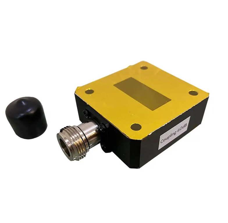
There are several types, each with its unique advantages. The microstrip coupler stands out for its compatibility with PCB technologies, offering ease of integration and cost-effectiveness, with production costs as low as $0.10 per unit in bulk. The stripline coupler, though bulkier, provides superior performance in terms of isolation and coupling accuracy, making it ideal for applications where space is not a constraint. Waveguide couplers offer the highest power handling capabilities, suitable for systems operating at power levels above 1 kW, but at a significantly higher cost, sometimes exceeding $1000 per unit.
Significance of Planarity in Directional Couplers
Planar directional couplers, such as microstrip and stripline, are crucial for modern electronics where space and weight are at a premium. Their planar nature allows for easy fabrication alongside other circuit elements on the same PCB, dramatically reducing assembly costs and improving reliability. The reduction in dimension is another key benefit, with some planar couplers measuring just a few millimeters across, facilitating integration into compact devices like smartphones and wearable technology.
The performance of planar couplers, particularly in terms of bandwidth and power handling, has seen significant improvements. Modern designs can handle bandwidths exceeding 40 GHz and power levels up to 50 Watts, meeting the demands of most contemporary applications. Achieving such performance requires precise control over material quality and fabrication processes, with deviations in substrate permittivity or conductor thickness potentially leading to performance degradation.

Design Considerations for Planar Directional Couplers
Material Selection
Choosing the right material is critical for the performance of planar directional couplers. Substrate materials such as FR4 are popular due to their low cost, around $2 per square foot, and adequate performance for non-critical applications. For high-frequency applications, advanced materials like Rogers 6002, despite a higher cost, approximately $25 per square foot, offer superior dielectric properties, leading to better efficiency and bandwidth performance.
Conductor materials also play a vital role. Copper is the most commonly used due to its excellent conductivity and cost-effectiveness, with prices around $0.50 per square inch for high-purity versions. Gold plating is sometimes applied to copper conductors to enhance corrosion resistance and reduce insertion loss, although this increases the cost significantly, potentially doubling the price of the conductor layer.
Geometric Configuration
The geometric design of a coupler impacts its coupling level, isolation, and directivity. A tighter coupling requires closer spacing between the conductors, which can increase the coupling efficiency but may lead to higher insertion loss if not properly managed. The optimal spacing typically ranges between 0.1 to 0.5 mm for microstrip couplers, balancing performance and manufacturability.
The length of the coupler determines the operational bandwidth. Longer couplers provide a broader bandwidth, with lengths of 10 to 20 wavelengths being common for ultra-wideband designs. This, however, increases the size of the component, making compact design a challenge.
Optimization for Planar Integration
Optimizing a directional coupler for planar integration involves balancing performance with integration requirements. Minimizing the footprint is essential for integration into densely packed circuits, necessitating innovative designs such as meander lines or spiral configurations. These designs can reduce the coupler’s size by up to 50% compared to straight-line configurations without significantly compromising performance.
Electromagnetic simulation tools are indispensable for optimizing planar directional couplers, enabling designers to predict performance accurately before physical prototypes are built. This approach saves time and cost by reducing the number of physical iterations required. The use of high-quality simulation software, though expensive, with licenses costing up to $30,000, can lead to significant cost savings in the development cycle by improving the quality and speed of design iterations.
Fabrication Techniques for Planar Directional Couplers
Photolithography for Planar Structures
Photolithography is a cornerstone in the fabrication of planar directional couplers, allowing for the precise patterning of conductive layers on a substrate. The process involves coating a substrate with a light-sensitive material, known as a photoresist, and then exposing it to ultraviolet light through a mask that defines the desired pattern. The accuracy of this technique is paramount, with feature resolutions down to 1 micron achievable, which is crucial for the high-frequency performance of the couplers.
The cost of photolithography equipment can be substantial, often exceeding $500,000 for systems capable of sub-micron precision. The investment in high-quality photolithography significantly improves the reliability and performance of the directional couplers, justifying the initial cost by reducing the need for costly reworks and increasing the yield of usable components.
Etching Processes
Following photolithography, the etching process removes the unwanted material to reveal the patterned conductor beneath. Wet etching, using chemical solutions to dissolve the excess material, offers a cost-effective method with material removal rates of approximately 0.1 to 1 micron per minute. For finer control and higher precision, dry etching techniques, reactive ion etching (RIE), are preferred, albeit at a higher cost due to the sophisticated equipment required, which can range from $100,000 to $500,000.
Dry etching provides superior edge definition and allows for the etching of denser and more complex patterns, essential for modern directional couplers where precision is crucial for minimizing insertion loss and achieving desired coupling levels.
Layer Deposition and Patterning
The deposition of conductive and dielectric layers is critical in building the multi-layer structures that planar directional couplers often require. Techniques sputtering and chemical vapor deposition (CVD) are widely used for their ability to create uniform and defect-free layers. Sputtering, can achieve layer thicknesses ranging from a few nanometers to several micrometers, allowing for precise control over the electrical properties of the coupler.
The costs associated with deposition equipment can be significant, with advanced CVD systems costing upwards of $1 million. The investment in high-quality deposition technologies ensures the longevity and performance of the directional couplers, particularly in terms of power handling and efficiency.
Each fabrication step, from photolithography to etching and deposition, plays a vital role in determining the final quality and performance of planar directional couplers. The choice of techniques and the precision with which they are executed directly impact the cost, efficiency, and reliability of these critical components. Balancing these factors is key to the successful fabrication of planar directional couplers that meet the demanding specifications of modern RF and microwave systems.


